|
3D Model |
Overlay |
Plan View |
|
|
|
|
|
|
|
|
|
|
|
|
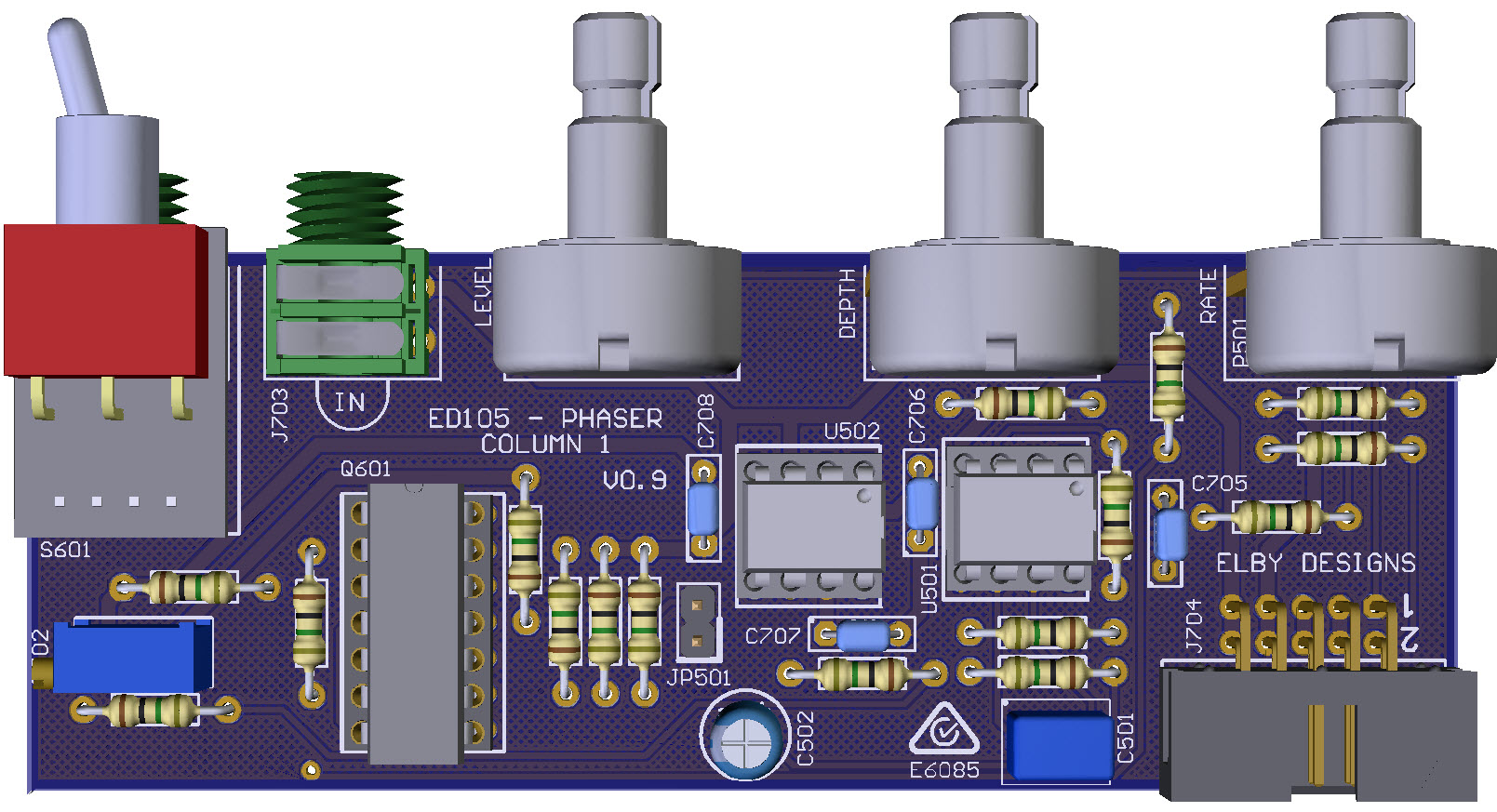
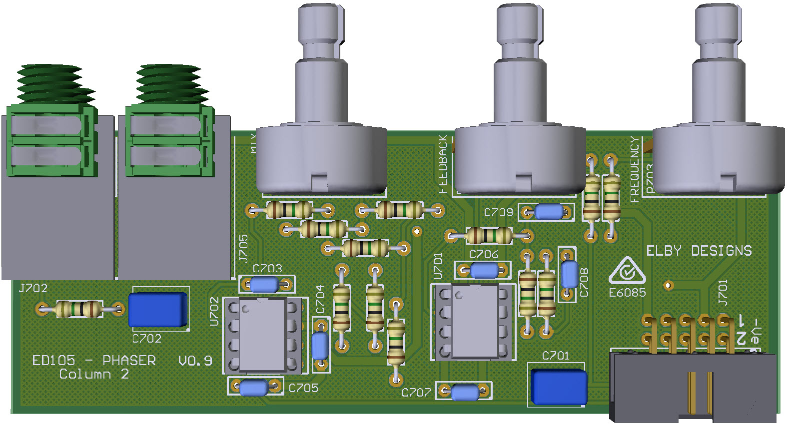
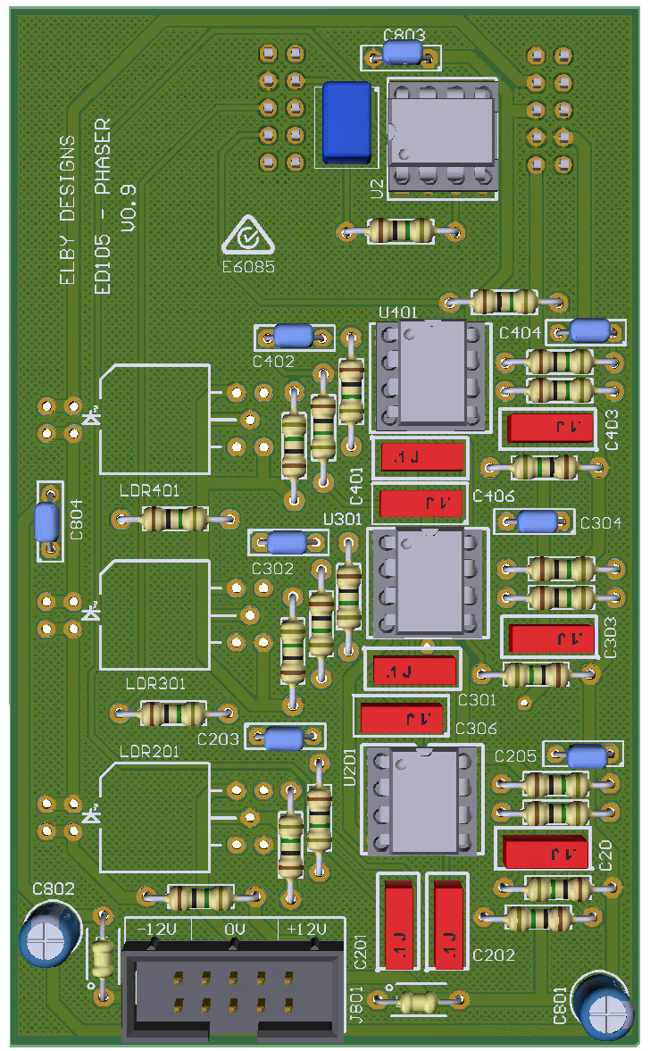
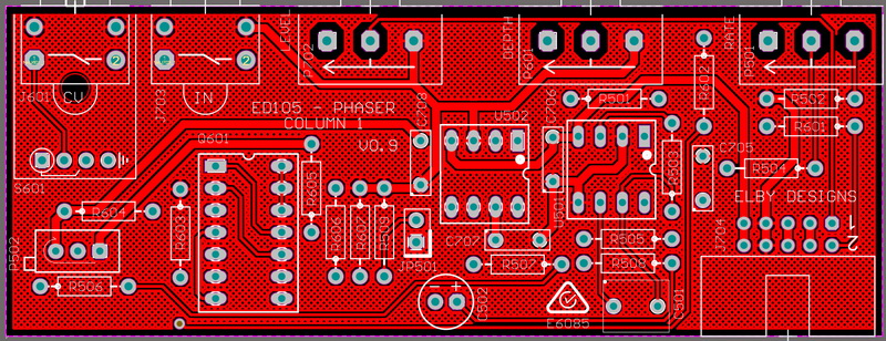
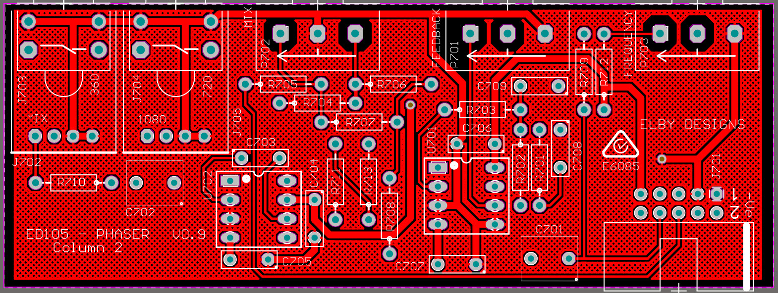
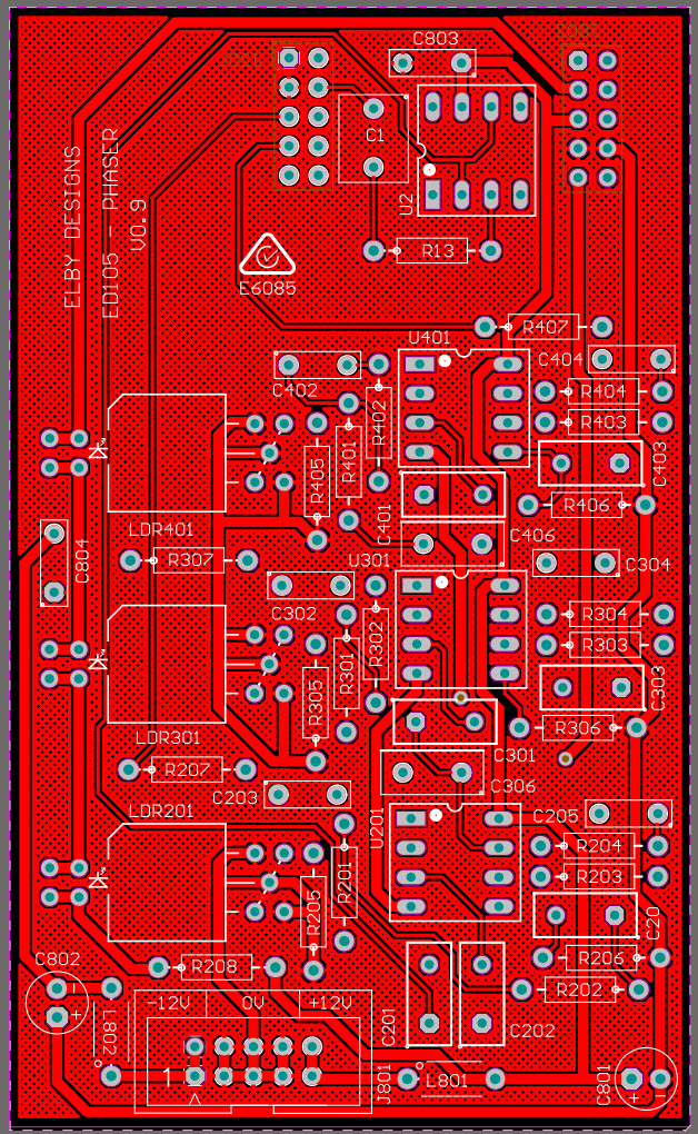
Constructors should refer to the Component Overlays along with,
the 3.5mm 4mm Bill Of Materials for the current value of all components, and
the General Construction Notes for general PCB assembly guidelines.
- Start by building the 3x Jack Carrier assemblies and 1x Switch Carrier assembly
- Fit all components to their respective PCBs except for the Carrier sub-assemblies
- Mount the Jack and Switch Carriers on to the Column 1 PCB but do not solder
- Offer the assembly up to the front panel and secure using the supplied nuts
- Check that the Switch Carrier is correctly aligned on the front panel so that the toggle goes up and down and then solder both Carrier assemblies
- Mount the Jack Carriers on to the Column 2 PCB but do not solder
- Offer the assembly up to the front panel and secure using the supplied nuts
- Solder both Carrier assemblies
- Mount the Main PCB ensuring that the IDC receptacles are correctly aligned with their respective IDC sockets