|
3D Model
|
Overlay
|
Plan View
|
|
|
|
|
|
|
|
|
|
|
|
|
|
|
|
|
|
|
|
|
|
|
|
|
|
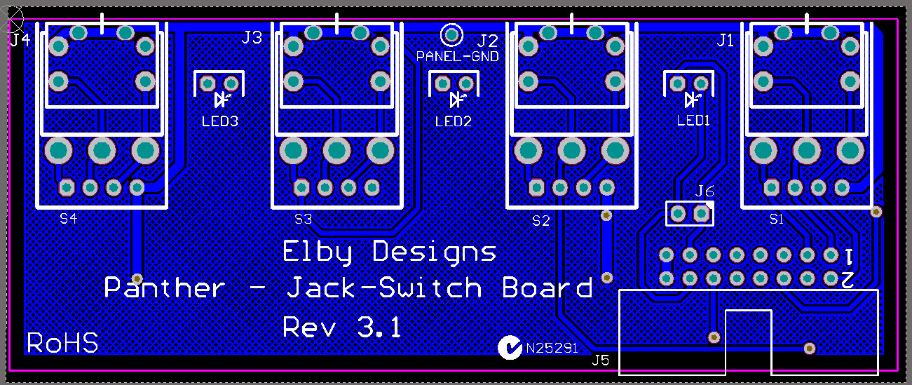
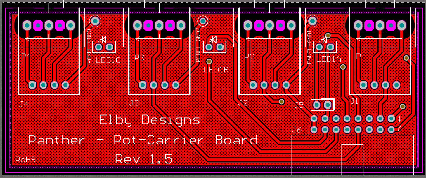
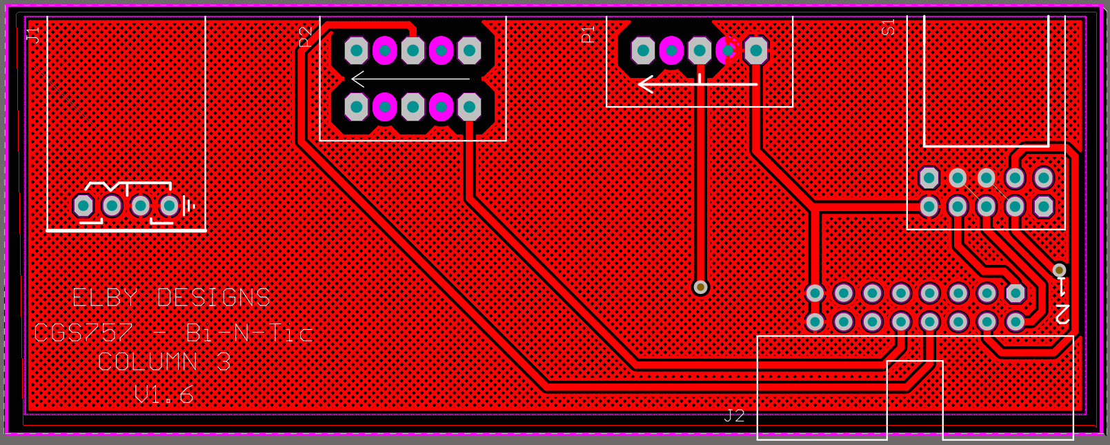
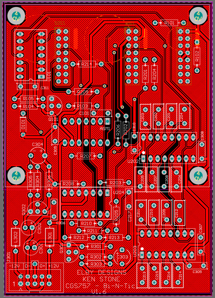
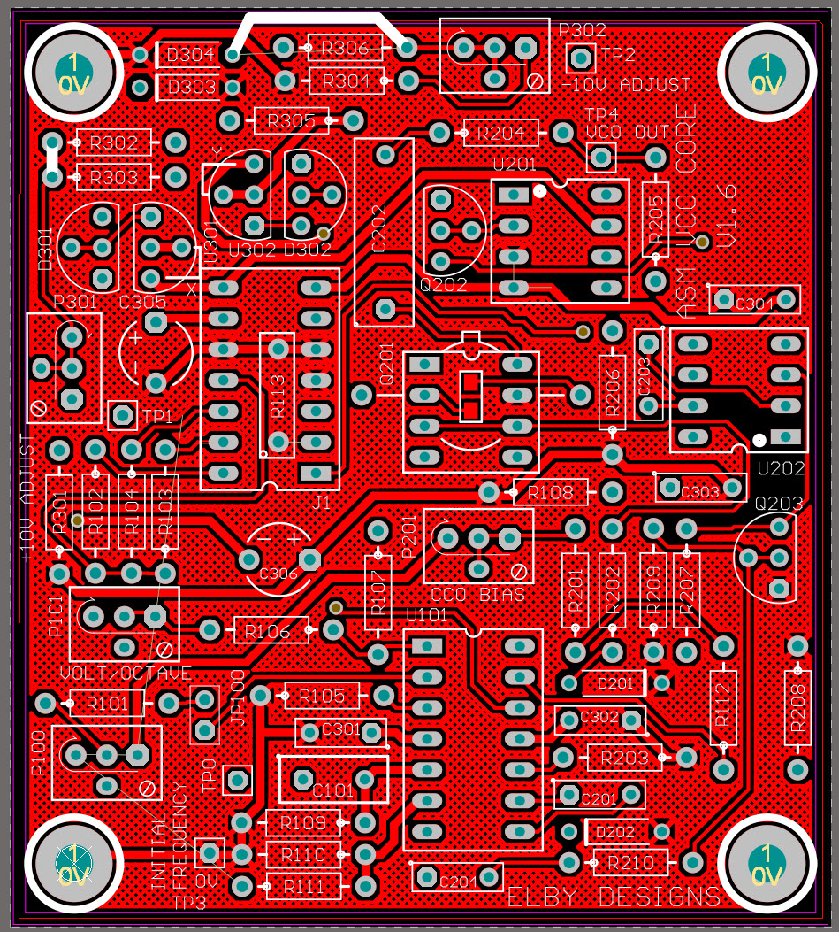
Constructors should refer to the Component Overlays along
with,
the Bill of
Materials for the current value of
all components, and
the General
Construction Notes for general PCB
assembly guidelines.
- Start
by assembling the 2x Jack Carrier boards
(3D
Model)
- Assemble
the Support PCBs
- Fit all components to Column 1
PCB
- Fit all components except the
jack sub-assembly to Column 2 PCB
- Fit all components except the
jack sub-assembly to Column 3 PCB
- Place
the jack sub-assembly on to the Column 2 PCB
assembly
- Offer
the sub-assembly up to the panel and secure
in place using the supplied nuts and washers
- Solder
the jack sub-assembly
- Repeat
for Column 3
- Fit
all components to the CGS757 main PCB except
for the wirewrap socket ASM1
- Fit
the 4x M3x12mm spacers using the M3x20mm
bolts
- Assemble
the ASM-VCO Core following its Build Guide
- Carefully
fit the wirewrap socket on to the header
pins on the underside of the ASM-1 Assembly
- Locate
the pins of the wirewrap socket in to its
footprint on the CGS757 board and secure the
ASM-1
- Assembly
using the 4x M3x6mm bolts
- Solder
the wirewrap pins and then cut to length
- Mount
the complete assembly on to the front panel
being careful to correctly align the IDC
connectors


