CGS359a - Assembly
CGS359b Assembly
|
-
Assemble all the PCBs excluding jacks, switches and LEDs
- Jacks and LEDs must be mounted on to the panel before attaching to the PCB. Once installed you will only be able to remove the boards by desoldering ALL of the panel components. Please triple-check all PCBs for solder/assembly issues BEFORE moving on to the next stage
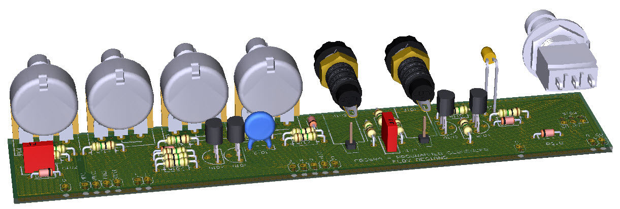
- Starting with the left-most CGS359A PCB (stage ‘1’)
- Cut 2x 10mm lengths of equipment wire and solder in to the pads for each jack on the PCB leaving around 8mm above the topside of the PCB
- Cut 2x 10mm lengths of equipment wire and solder in to the pads for the switch on the PCB leaving about 5mm above the topside of the PCB
- Mount the associated jacks on to the front panel
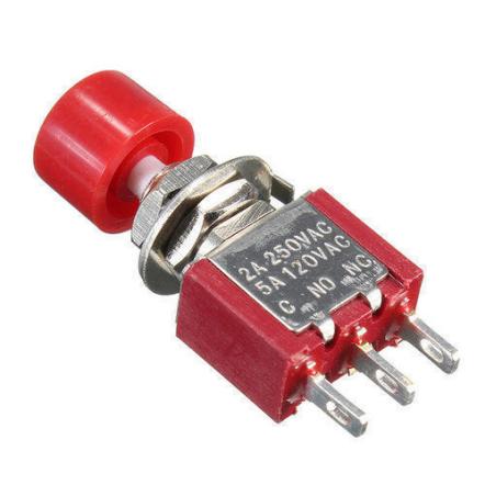
- Mount the associated switch on to the front panel keeping the longer length of the body vertical. Make sure that the ‘CO’ leg of the switch (marked on the body moulding) aligns with the ‘CO’ pad on the PCB
- Mount the associated LED lens on to the front panel with the ANODE (longer leg) vertically at the top
- Offer the PCB up to the front panel and secure the pots using the supplied nuts and washers
- Carefully form the LED legs and insert in to the footprint on the PCB. You may need to fold in a kink to ensure that no more than a couple of mm of leg poke through the underside
- Top solder the LED legs in to place
- Feed the wire for each jack through its associated mounting hole on the jack and solder in to place
- Solder the wires to the switch. If using a 2-pin SPST switch then wire the pins to the 2 left pads (nearest the centre of the PCB) marked ‘CO’ and ‘NO’
- Repeat steps (4) to(13) for the remaining CGS359A in the system
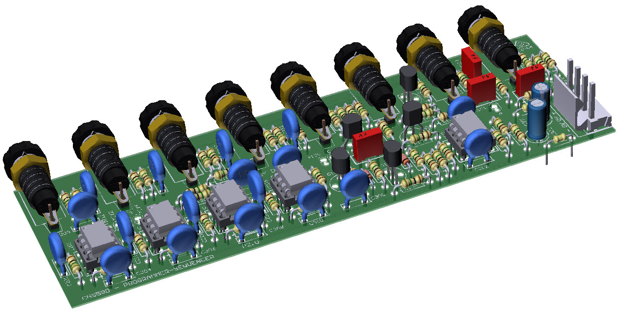
- Install the jacks for the CGS359B
- Cut 2x 8mm lengths of equipment wire and solder in to the pads for each jack on the PCB
- Offer the CGS359B up to the panel, feeding the wires through the jack mounting pots.
- Holding the PCB firmly against the jack bodies, solder the jacks in to place.
- Using appropriate lengths of tinned copper wire, feed the wire through the link position ‘G’ on the ‘1st STAGE’ CGS359A and in to the ‘H’ link position on the ‘2nd Stage’ CGS359A and terminate in ‘J’ link position on the ‘3rd Stage’ CGS359A
- Repeat step (19) but this time start with link position ‘G’ on the ‘2nd Stage’ CGS359A terminating at link position ‘J’ on the ‘5th Stage’ CGS359A
- When you reach the last stages of the unit, wrap around to the beginning stages following the same ‘G’ – ‘H’ – ‘J’ pattern.
- Using appropriate lengths of tinned copper wire, feed the wire through the link position ‘C’ on all PCBs (CGS359A and CGS359B) and solder in to position on each PCB
- Repeat step (22) for all the remaining link positions (MIX1, MIX2, MIX3, MIX4, E, F, +12V, D, A, B and 0V
|
|
|


