| |
|
3D Model |
Overlay |
Plan View |
PCB |
|
|
|
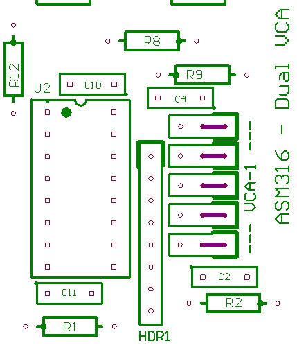
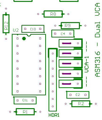
Constructors should refer to the Component Overlays along with,
the Bill of Materials for the current value of all components, and
the General Construction Notes for general PCB assembly guidelines.
- Assemble the 2x Jack Carrier boards
- Assemble the 2x Switch Carrier boards
- Fit all components to the boards except for all the sub-assemblies, HDR1 and the 5x jumpers
- For Column 1, fit wire links in the position marked ‘VCA-1‘
- For Column 2, fit the links in the opposite positions
- Mount the 2x sub-assemblies to the Column 2 board but do not solder
- Offer the assembly up to the front panel and secure the using the supplied nuts and washers
- Solder the sub-assemblies in to place
- Remove the Column 2 assembly
- Mount the 2x sub-assemblies to the Column 1 board but do not solder
- Offer the assembly up to the front panel and secure using the supplied nuts and washers
- Solder the sub-assemblies in to place
- Insert and solder HDR1 in to its location on the Column 1 assembly
- Carefully fold HDR1 in to a concertina shape
- Offer the Column 2 assembly up to the front panel while carefully inserting the pins on HDR1 in to their location on the underside of Column 2
- With Column 2 installed and secured, and HDR1 sitting correctly, solder it in to position.
|
|
|